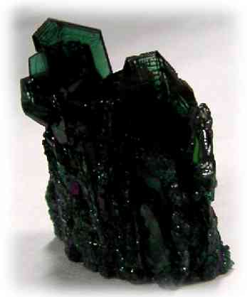
| Have you ever heard the phrase of "wide gap semiconductor"? The wide gap semiconductor means semiconductor with wide "energy gap", which greatly represents semiconductor property. Silicon, which is the most popular semiconductor material, has an energy gap of 1.1 eV. On the other hand, representative wide gap semiconductors such as silicon carbide (SiC) and galium nitride (GaN) have energy gaps of larger than 2.0 eV. The wide gap semiconductors are transparent crystal due to these large band gaps, and because of difficultly for crystal synthesis it have been considered that realization of wide gap semiconductor devices is also difficult. However, in past decades, progress for crystal growth of these materials makes research for wide gap semiconductor devices aggressive. |
|
|
|
|
|
|
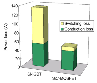
The most promising application of SiC is usage as a materials for power devices, which can control electricity with high power densities. At present, power devices are usually fabricated by Si, but Si has a limit in the highest controllable power density. Therefore, realization of SiC power devices is anticipated. By the way, where are the power devices employed in our life? In fact they are employed in motor inverters for electrical trains and vehicles, air conditioners and so on. They are also employed in voltage controllers in electric power networks. SiC power device can reduce more than 1% in carbon dioxide emission. In addition, because of high thermal conductivity of wide gap semiconductors, volume of power modules can decrease which leads increase of space efficiency and reduction of its weight. |
|
|
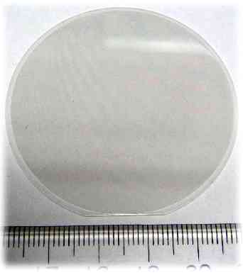
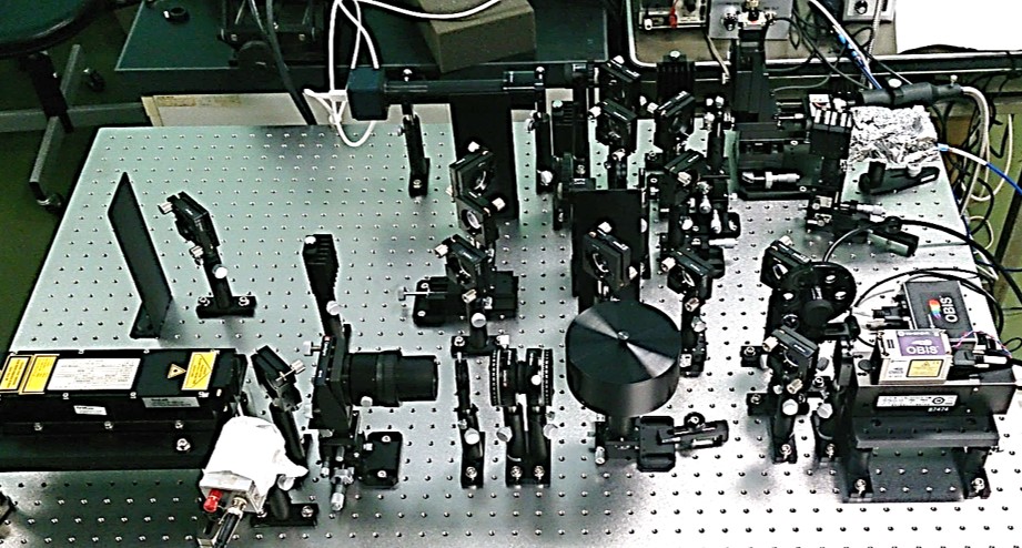
| However, we still have many hardles for realization of wide gap semiconductor devices. For example, densities of crystalline defect are high in SiC compared with Si, so the defects degrade performance of SiC devices. SiC wafers are small compared with Si, and thus costs of SiC device are relatively high. To overcome these problems, we are studying characteristics of crystalline defects in SiC and techniques to suppress negative influence of the defects. We are also developing characterization and processing systems in order to contribute realization of wide gap semiconductor devices. |
|
|
|